
IISc Bangalore: Arjun’s Dream Unfolds
Arjun Vijayan of Class 12, Bharata Matha Higher Secondary School, Palakkad, Kerala, recently visited the Indian Institute of Science, Bangalore as part of a small group of 15 students. He shares his experience, in his own words, here.
AIM
This study trip to the Indian Institute of Science was conducted by the Bharathamatha Alumni Association (BASS) on to provide aspiring students, a special opportunity to visit, explore and gain knowledge from one of the most reputed institutions in India, IISc (Indian Institute of Science) Bangalore.
IISc is famous for its contribution to many renowned scientists like Sudha Murthy and Dr. C V Raman. This program helped students to gain a deeper knowledge of the scientific advancements and research done by the students and teachers, for the well being of the society.
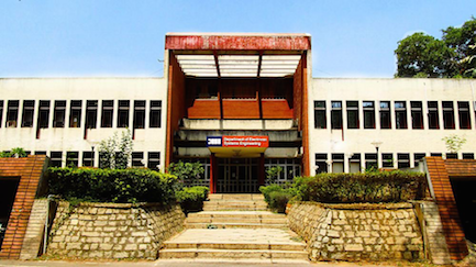
ABOUT- IISc Bangalore
IISc is a public institute deemed to be a university for research and higher education in science and engineering, located in Bangalore in the Indian state of Karnataka.
The institute was established in 1909 with active support from Jamsetji Tata and Krishna Raja Wadiyar IV and thus is also locally known as the “Tata Institute”. It was granted the deemed to be university status in 1958 and the Institute of Eminence status in 2018. The IISc campus is located in the north of Bengaluru, about 4 kilometers from Bangalore City Railway Station and Kempegowda Bus Station, on the way to Yeshwantpur.
PLACES VISITED
As a part of the study trip, I visited
- Electronic and System Packaging Lab
- CeNSE
- Nano Technology Lab
- National Nano Fabrication Centre
- Incubation Centre, IISc
ELECTRONIC AND SYSTEM PACKAGING LAB
Electronic and System Packaging Lab in IISc mainly does its research on possible improvements in PCB (Printed Circuit Boards). They make PCB through a complex process in order to run tests on them and make solutions that benefit humankind.
This faculty produces Double Layered PCB’s about the thickness of 1.6mm, which are exclusively used for research purposes. They cover the PCB with photoresist material and then pass it through UV radiations, which removes the glass epoxy from exposed regions in the layer. Tracks are made and components are soldered using Soldering Paste. The complete process and Mechanism of System Packaging was explained by Mrs. K B Vasantha, Sir Antony and Sir G V Mahesh.
CeNSE-CENTRE FOR NANOSCIENCE AND ENGINEERING
The Centre for Nano Science and Engineering (CeNSE) was established in 2010 to pursue interdisciplinary research across different branches of Nano Technology. The state of the art faculty was inaugurated by PM Shri. Narendra Modi, and since then CeNSE had been one of the leading and most successful Nanotech research laboratories in India.
CeNSE consists of two main faculties:
- Nano Technology Lab
- National Nanofabrication Centre
NANOTECHNOLOGY LAB
The Nano Technology Lab at IISc Bangalore does its research and characterizes in three fundamental aspects of a material-Electrical characterization, Mechanical characterization and optical characterization.
The Material Characterization facility deals with the measurements, quantity and the physical properties of a given substance at a molecular level, like the surface thickness, density etc. They use equipments like Optical profilometer, Atomic force microscope and the scanning acoustic microscope to find damages and to study physical properties of substances.
Optical characterization facility includes a transmission electron microscope which is used to study different mechanisms and properties at a subatomic level and is used to study surface morphology and presence of certain elements.
Electrical Characterization facility is used to determine resistivity, carrier concentration, mobility, contact resistance, barrier height, depletion width, oxide charge, interface states, carrier lifetimes, and deep level impurities.
NATIONAL NANO FABRICATION CENTRE
The National Nano Fabrication Centre at IISc Bangalore is basically one of the few cleanrooms developed in India to make valuable research on sub-atomic particles, and on Integrated Circuit Development. This faculty seemed to be a Nanoscale application faculty for the research developed on a macro scale at the System Packaging Lab as explained to us by Chandan Sir.
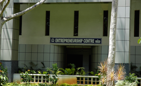
SID (INCUBATION CENTRE)
This state of the art facility, funded by Bosch Ltd. promotes valuable development and innovations by funding several startup programs that would be of great use for the well-being of the society.
Lab to Market is a startup program run by Prof. S K Sinhala in order to improve the current condition of railways and to make them more efficient.
Lab to market is designing an optical-fiber grating technology, which can be used to make miniature-sized sensors that can detect and identify trains and send information to necessary sources.
Similarly, a group of scientists, Mr. Hashish, Rojas and Adyta, are developing drone mechanisms to self-charge it on a given platform by itself, which could be of great importance as the age of automated drones has come to rise.
Mr. Adyta is developing an AI-powered dog that self learns to walk and understand simple commands. Mr. Rokass is in charge of the state of the art 3D printing facility which supports and provides the facility with necessary parts.
CONCLUSION
I owe my sincere thanks to Bharathamatha HSS and its alumni association in selecting me in this fascinating and eye-opening trip to one of the most reputed institutions in India, the IISc.
I was able to gain knowledge and understand more about the scientific advancements in our world and how we can be a part of it. This trip aspired me to work harder and make my own contribution to the scientific world.
I also owe my sincere thanks to Rev Fr Paul Thekkiniyath, Smitha Teacher, Sajna Teacher and Alumni Association Convenor Mr.Dileep for providing me support and for playing an important role in this study tour.
Curious Times is a leading newspaper and website for kids. We publish daily global news aligned to your learning levels (also as per NEP 2020): Foundational, Preparatory (Primary), Middle and Senior. So, check out the News tab for this. We bring kids’ favourite Curious Times Weekly newspaper every weekend with top news, feature stories and kids’ contributions. Check out daily JokesPoke, Tongue Twisters, Word of the Day and Quote of the Day, kids need it all the time.
ME – My Expressions at Curious Times is your place to get your work published, building your quality digital footprint. And it is a good way to share your talent and skills with your friends, family, school, teachers and the world. Thus, as you will step into higher educational institutes your published content will showcase your strength.
Events, Quizzes and Competitions bring students from over 5,000 schools globally to participate in the 21st-Century themes. Here schools and students win certificates, prizes and recognition through these global events.
Sign-up for your school for FREE!
Communicate with us: WhatsApp, Instagram, Facebook, Youtube, Twitter, and LinkedIn.
0 (Please login to give a Curious Clap to your friend.)
SignUp to Participate Now! Win Certifiates and Prizes.
Login/Signup